It is a common practice to have multiple copies of the same PCB on a bigger PCB, so that you can handle many small boards as one bigger board. Usually, there are perforated snap-offs separating each board. This big board is called a panel. To assemble a panel, one option is to have the CAD system to generate a pick and place file that has all the sub-board information. With this method, the LitePlacer software doesn’t even know it is assembling a panel instead of a single design.
If your CAD system does not support panelizing, the LitePlacer software has function for this. First, load the CAD data file representing a single board design. Then, click the “Panelize” button, and this form appears:
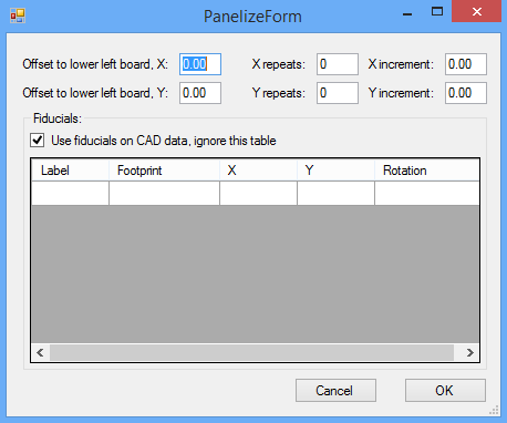
Here, you input the measures of the panel. Here is a sketch:
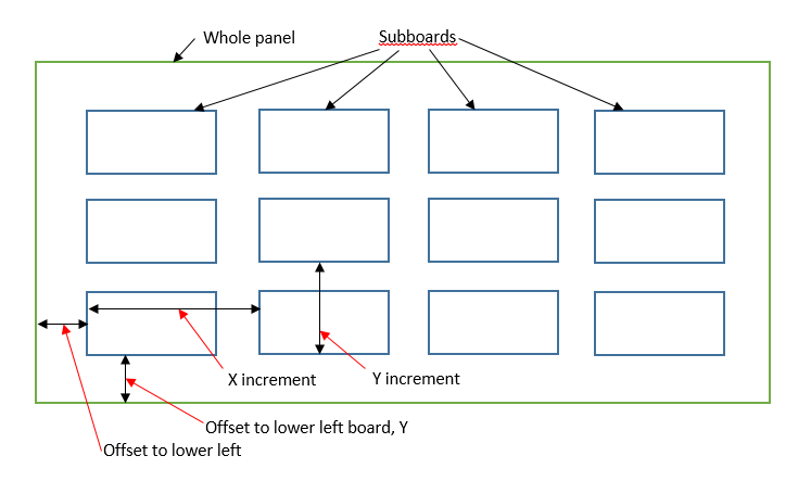
The offsets tell the panel edge thickness, and the increments are the distance of the individual board origos, in mm’s. The repeats tell the number of individual subboards, in this case, X repeats is 4 and Y repeats is 3.
Sometimes, there are no fiducials on the subboards, but on the panel edge. For this, you can input the nominal coordinates of the fiducials to the table at the bottom of the form. If you check the box (checked in the example), the software assumes there are fiducials on the individual subboards and uses them. If you have at least two repeats on each direction, you need only one fiducial on each board; the software gets the four fiducials it needs (see PCB requirements).
When you click “OK”, the software builds a CAD file representing the whole panel to the CAD data table. Save the data! This process also creates corresponding job data, as usual.